Signal Processing
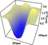
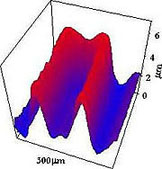
The figures to the right show a 300 x 400 µm2 section of an
operational transistor imaged using a 0.1 mm diameter Pt tip. The bias potential
changes are clearly visible through the native oxide layer above a single pn
junction, together with the associated topographic image.
One major problem associated with the null method is
obviously the low signal to noise level at balance. Together with co-workers at Twente University in the Netherlands I developed an 'off-null' approach. Here Vb
is derived from a computer steered digital-to-analogue converter which is set to
a range of potentials around the balance point. At each value Vptp is
determined: a plot of Vptrp versus Vb is thus a straight line, the intersection
with the Vb axis producing Vc. In this fashion changes in Vc can be determined
to sub-mV resolution.
An advantage of this 'off-null' method is that measurements
are performed on high signal levels and the balance point is determined via
extrapolation. A further benefit is that the gradient of the Vptp versus Vb line
is very sensitive to changes in mean spacing and can be used to maintain a
constant spacing either during an experiment or throughout a scan. In this
fashion the KP can map out surface potential changes simultaneously with sub-
micron scale sample topography.
|

Single Electron Transistor Device results scan
Kelvin Probe 50micron tip measuring a Single Electron Transistor Device
Scanning Kelvin Probe
UHV Kelvin Probe
Solar Panels
Scanning Kelvin Probe
|


