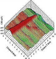
 This is a Kelvin Probe scan of a SiO2 passivated
multicrystalline Solar Cell showing bus bar, silver fingers and semiconductor regions.
This is a Kelvin Probe scan of a SiO2 passivated
multicrystalline Solar Cell showing bus bar, silver fingers and semiconductor regions.
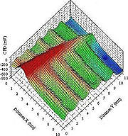 This scan is of a Si3N4 passivated Solar Cell.
This is a higher performance cell than the SiO2 coated one due to the gettering effect of hydrogen on bulk traps.
The Silicon surface is much smoother and the open circuit voltage (measured with the Kelvin probe) is much larger.
This scan is of a Si3N4 passivated Solar Cell.
This is a higher performance cell than the SiO2 coated one due to the gettering effect of hydrogen on bulk traps.
The Silicon surface is much smoother and the open circuit voltage (measured with the Kelvin probe) is much larger.
Investigating Solar Cells with the Kelvin Probe
We are currently using the Scanning Kelvin Probes with tips of diameter 0.15-0.5 mm to scan the front surface of semiconductor solar cell materials.
The resulting surface potential topographies provide information on the quality of the front electrical contact; the electrical characteristics of
the buried pn junction; the surface interface traps and the effects of varying light energy and intensity.
Such multi-crystalline cells are not highly
efficient and this study produces information on the surface traps, recombination centers and degradation of cell performance with temperature. Via appropriate
biasing technique the Kelvin Probe can selectively provide information on the surface and/or the bulk phenomena. This data can be used to optimise solar cell
efficiency.The diagrams show the front electrical contact composed of silver bus-bar (coloured red) and associated fingers.
These contacts are screen printed
on top of a thin layer (60 nm) of either SiO2 or Si3N4 passivation. Avrid van der Heide, ECN Petten, The Netherlands has kindly supplied these samples. We observe
that the electrical contact between the silver layer and the underlying, highly-doped emitter layer (100 nm thick) is excellent, indicating that the drive-in
diffusion of silver through the passivation was successful. Further SKP scans and point measurements performed under dark and white light illumination, termed
the surface photovoltage (see the SPV section on this website) clearly show that the charge trapping lifetimes in the interface between the two type of surface
passivation is completely different.
Further we can show, via a non-contact surface potential measurement that the open circuit voltage degrades with temperature.
In this fashion we can directly measure the changes in sub-surface quasi fermi-level as a function of light intensity and thus provide information on how the cell
responds to different light intensities.
|

Single Electron Transistor Device results scan
Kelvin Probe 50micron tip measuring a Single Electron Transistor Device
Scanning Kelvin Probe
UHV Kelvin Probe
Solar Panels
Scanning Kelvin Probe
|