|
|
|||||||||
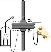 The original apparatus of Lord Kelvin.  Cr deposited on Si(100) Sample courtesy of Dr. Bert Lagel, University of South Florida.  100nm ITO on glass - Sample courtesy of Dr. Dmitry Poplavskyy, OSRAM Opto Semiconductors Inc  100nm PEDOT:PSS - Sample courtesy of Dr. Dmitry Poplavskyy, OSRAM Opto Semiconductors Inc. Welcome to the Kelvin Probe information site
The Kelvin Probe is a non-contact, non-destructive measurement device used to investigate properties of materials. Ideas and examples
This website provides information on the science behind the Kelvin Probe, ideas for applications, examples of measurements and some comments on current apparatus available.
All are compiled by Professor Iain D. Baikie who has extensive experience in the technique. Kelvin Probe Webinar, World Wide BroadcastFebruary 2010 In February 2010 Professor Iain Baikie in conjunction with the publication 'Thin Solid Film' headed up an expert panel presenting an educational webinar introducing viewers to the principle of the Kelvin Probe technique, explaining how it works, the information it provides and how this can be interpreted through the use of examples and typical applications in Materials Science. Attendees discovered the advantages this highly sensitive research tool can offer and had the opportunity to ask any questions relevant to the Kelvin Probe technique and their current research requirements. A recording of this event is now available to watch at your leisure: Introduction to the Traditional Kelvin Probe for High Resolution Work Function Measurements recorded live on Thursday 25th February 
|
|
| KP Technology Ltd., Burn Street, Wick, Caithness, Scotland, KW1 5EH. Tel: + 44(0)1955 602777 | Contact |