Semiconductors
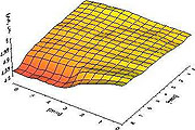
An example of an in-situ work function topography of a clean
Si(111) 7x7 single crystal is shown here. The work function is mostly flat with
a depression in one area which is in the vicinity of the sample contact. Using
optical pyrometry we can determine that this region of the sample was 50 ºC
cooler and subsequent AES analysis indicated a modest build-up of carbon
contamination (< 10%).
The Kelvin Probe has been used to study in detail the
oxidation of Si surfaces which serves as a reminder of the sensitivity of the
method. As the induced surface dipole at monolayer (ML) coverage is quite large-
upwards of 1 V-, sub-mV work function accuracy infers resolutions of
approximately 1/1000 ML in coverage. STM and AES can also be used to follow this
reaction however STM topographies quickly become confused at relatively low
coverage, e.g., > 0.1 ML and it is very difficult to obtain accurate chemical
information below 0.3 ML. The KP data however are continuous throughout this
region and offer additional information regarding atomic re-arrangements,
density of surface states, etc.
We have employed similar measurements on polycrystalline
metals such as Re and W in order to follow their high temperature (800 - 1400 oC)
oxidation characteristics. The resulting high work function surface, i.e., >7 eV,
will be used as positive ion sources.
|

Single Electron Transistor Device results scan
Kelvin Probe 50micron tip measuring a Single Electron Transistor Device
Scanning Kelvin Probe
UHV Kelvin Probe
Solar Panels
Scanning Kelvin Probe
|